Chip science explainer
IBM Sub-1 Nanometer Chip Explained: What 0.7 nm Really Means
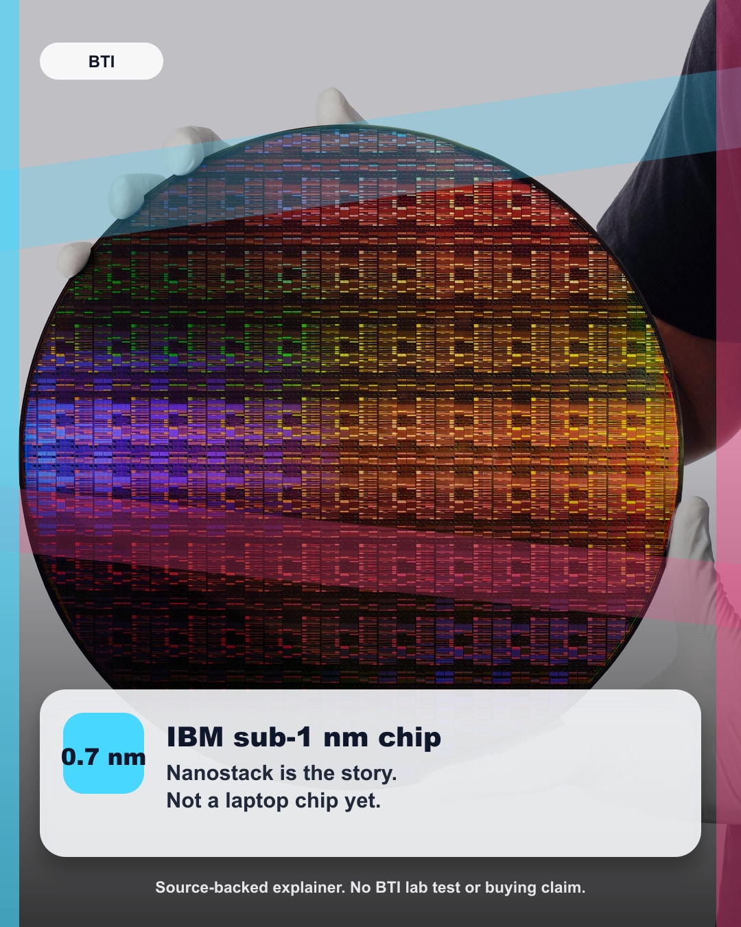
The simple version: IBM’s 0.7 nm story is about stacking transistor structure at atomic scale, not a laptop chip you can buy today.
The IBM sub-1 nanometer chip story sounds like science fiction because the number is so small. IBM announced sub-1 nm chip technology at the 0.7 nm, or 7 angstrom, node. The normal-reader version is simpler: IBM is showing a new way to keep packing more useful transistor structure into a chip as traditional flat scaling gets harder.
The key word is nanostack. Instead of treating the chip only as a flat layer of tiny switches, IBM describes a three-dimensional transistor architecture that vertically stacks and staggers transistor layers. That is why this is a good BTI explainer topic. It turns a difficult semiconductor announcement into a visual idea: when the floor gets crowded, chip designers start thinking upward.
BTI has not tested an IBM sub-1 nm chip, inspected IBM’s lab results, audited manufacturing readiness, or verified performance, power, yield, price, product timing, or customer deployment. This guide translates public source material and keeps the claim boundaries visible.
- 0.7 nm is a future chip-node story, not a promise that buyers can shop for a finished device today.
- IBM says the design can pack nearly 100 billion transistors into a fingernail-sized chip area.
- The useful buyer takeaway is patience: this explains where chips may go, not what laptop to buy this morning.
IBM sub-1 nanometer chip quick answer
The IBM sub-1 nanometer chip is a research milestone built around IBM’s nanostack transistor architecture. IBM says the 0.7 nm node could offer up to 50 percent more performance or 70 percent greater energy efficiency than IBM’s 2 nm node chips, and that it sees a path to production in as early as five years. Treat those as source-backed IBM statements, not independent BTI testing.
The best beginner mental model is a city skyline. If the ground is full, builders add height. Nanostack applies that kind of vertical thinking to transistor architecture. It does not make the physics easy, but it gives normal readers a way to understand why 3D chip structure matters.
| Term | Plain-English meaning | Safe read |
|---|---|---|
| 0.7 nm / 7 angstrom node | A research node label for a future chip-making generation, not a ruler measurement of one whole chip. | Use it as a density and architecture story, not as proof that a consumer device has launched. |
| Nanostack | IBM’s three-dimensional transistor architecture that stacks and staggers transistor layers. | The beginner idea is vertical packing: more useful transistor structure in the same chip area. |
| Nearly 100 billion transistors | IBM says the research chip can pack nearly 100 billion transistor switches into a fingernail-sized area. | That is the mental image readers should remember, while keeping it tied to IBM’s source material. |
| SRAM scaling | SRAM is fast on-chip memory that helps processors keep important data close. | IBM says its VLSI 2026 research showed 40 percent SRAM scaling; do not turn that into a laptop benchmark. |
| Path to production | IBM says it sees a path to production in as early as the next five years. | That is a roadmap statement, not a product launch, price, pre-order, or buying recommendation. |
Why IBM’s 0.7 nm chip story matters
Modern chips depend on transistors, the tiny electronic switches that help processors calculate, remember, and move information. For decades, the industry improved chips partly by shrinking and packing those switches more densely. But as chip features approach atomic dimensions, old scaling tricks become harder to keep using.
That is the context for IBM’s announcement. IBM says its sub-1 nm technology uses structural and material innovations, including nanostack, to keep density and efficiency gains moving. The headline number is attention-grabbing, but the deeper story is architecture. IBM is saying that chip progress can continue by changing how transistors are arranged, not merely by shrinking a flat design.
The AI angle is also real, but it needs careful wording. Generative AI and cloud infrastructure need enormous compute. More efficient chips could help future systems do more work per watt. That does not mean today’s AI data centers instantly become 70 percent more efficient, and it does not mean every future processor will use this exact design. It means the research direction matters for the next decade of hardware.
What 0.7 nm actually means
A nanometer is one billionth of a meter, but chip-node names are not simple ruler measurements. The number is a generation label that points to the density, architecture, and manufacturing era of a technology. That is why the safe BTI phrasing is “0.7 nm node” or “7 angstrom node,” not “every feature on the chip is exactly 0.7 nm.”
IBM’s own announcement says transistor nodes now refer to a generation of manufacturing technology versus an exact physical dimension. That sentence is important for a viral explainer because it prevents the biggest misunderstanding. The magic is not that the whole chip is 0.7 nm. The story is that IBM is showing a way to extend logic scaling below the 1 nm node.
For a normal reader, the easiest translation is this: the smaller node story is really a density story. More transistor structure can fit into a familiar chip area, which can create room for better performance, better efficiency, or more capable compute systems if the technology eventually manufactures well at scale.
Why nanostack is the useful word
Nanostack is IBM’s name for the new three-dimensional transistor architecture. IBM describes it as a nanosheet-based design that vertically stacks and staggers transistors. The design also allows different material combinations in each stacked layer, which IBM says can help optimize power and performance independently.
That is a mouthful, so here is the beginner version: chip designers are trying to use height, structure, and materials more intelligently. Instead of only making the footprint smaller, nanostack changes the arrangement. That is why a good Instagram frame should not say “tiny chip magic.” It should say “chips may start building upward.”
IBM also says the architecture was experimentally validated through dielectric bonding, dual-channel engineering, and functional CMOS inverter operation. BTI should not pretend those are consumer features. They are evidence that IBM is presenting this as physically buildable research, not just a concept slide.
What IBM says vs what readers should not overclaim
This is the slide that makes the story trustworthy. The IBM sub-1 nanometer chip announcement has big numbers, but each number needs a safe interpretation.
| Source point | What it means | Do not assume |
|---|---|---|
| Up to 50 percent more performance | IBM describes a projected capability compared with IBM’s 2 nm node chips. | Do not call it an independent BTI benchmark, a finished product result, or a guaranteed device speedup. |
| 70 percent greater energy efficiency | IBM frames this as a projected efficiency improvement versus IBM’s 2 nm node chips. | Do not promise lower power bills for current laptops, phones, servers, or AI services. |
| Nearly 100 billion transistors | The useful mental model is density: many more electronic switches in a fingernail-sized chip area. | Do not say BTI inspected the chip, verified density, or tested a finished commercial processor. |
| Production in as early as five years | IBM is describing a possible route from research toward manufacturing. | Do not write that buyers can shop for a sub-1 nm IBM laptop chip now. |
Why this is not a laptop buying guide yet
It is tempting to turn every chip headline into a shopping tip. That would be wrong here. IBM’s sub-1 nm chip technology is research and roadmap material. IBM says it sees a path to production in as early as the next five years. That puts the story in the “watch this future direction” bucket, not the “buy this product now” bucket.
For buyers, the practical rule is simple. If you need a laptop, phone, console, or workstation now, buy based on real products, memory, battery life, ports, thermals, app support, and return policy. If you enjoy chip science, save this as a marker for where the industry may head after 2 nm and 1.4 nm discussions.
That distinction is part of BTI’s value. A hype account can make every lab result sound like a product launch. A useful explainer tells you what changed, why it matters, what is still research, and what not to buy or believe yet.
Why AI makes the IBM chip story easier to care about
AI has made chip power easier for normal people to notice. Every chatbot answer, image model, coding assistant, and agent workflow depends on data centers, accelerators, memory, networking, cooling, and electricity. If future logic and memory structures can do more work per watt, the impact could reach cloud services and AI infrastructure over time.
IBM’s announcement names generative AI and cloud infrastructure as possible application areas. The safer BTI read is not “this solves AI power.” It is “this shows one research path for future compute density and efficiency.” That is still interesting. It explains why the chip industry cares about atomic-scale architecture even when most buyers never see the silicon.
For Instagram, this topic should be framed as a science breakdown, not a shopping recommendation. The first frame can ask: “Did IBM just go below 1 nm?” The middle frames should explain node names, nanostack, transistor density, and the five-year production path. The final frame should tell readers to save the chart before the next chip headline.
Sources for this IBM sub-1 nm chip guide
BTI used public source material and did not perform lab testing, manufacturing analysis, product testing, performance benchmarking, price research, stock analysis, or availability checks for this guide.
- IBM newsroom announcement: The official June 25, 2026 source for the 0.7 nm node, nanostack architecture, transistor-density claim, VLSI references, and production-path wording.
- TechXplore report: Summarizes the same IBM announcement and adds a plain-language reminder that node labels do not mean a literal chip-part measurement.
- Times Union Albany NanoTech report: Local reporting ties the work to Albany NanoTech and repeats the nanostack and nearly 100 billion transistor framing.
What not to overclaim
Do not treat IBM’s 0.7 nm node announcement as proof that current devices will suddenly get the same performance, power, or battery-life gains. IBM is describing a research technology direction and projected node-level improvements compared with IBM’s 2 nm node, not a BTI-tested consumer chip.
Do not turn this into market advice, a brand endorsement, or a buying recommendation. The clean BTI angle is educational: explain node names, show why nanostack is different, and separate the lab milestone from anything buyers can evaluate in a finished product.
IBM sub-1 nanometer chip FAQ
Is IBM’s sub-1 nanometer chip a real product I can buy?
No. IBM describes this as chip technology and a path toward production, not a consumer product you can buy today.
Does 0.7 nm mean every chip part is exactly 0.7 nanometers?
No. IBM says transistor nodes now refer to a generation of manufacturing technology rather than an exact physical dimension.
What is nanostack?
Nanostack is IBM’s three-dimensional transistor architecture that stacks and staggers transistor layers to keep chip scaling moving below the 1 nm node.
Should this change what laptop I buy right now?
No. Treat it as a future chip-science milestone. Buy current devices based on published specs, your workload, repair support, and the return policy.
Evidence BTI used
The core evidence is IBM’s June 25, 2026 announcement, which gives the 0.7 nm node, nanostack architecture, nearly 100 billion transistor framing, SRAM scaling reference, projected performance and efficiency language, and production-path wording. BTI cross-checked the plain-English framing with TechXplore and local Albany NanoTech reporting from the Times Union.
Because the evidence is public source material, this article uses cautious verbs: IBM says, IBM describes, and IBM sees a path. BTI is not independently verifying the lab work or predicting when finished devices will use this technology.
BTI final take
The IBM sub-1 nanometer chip story is interesting because it gives normal readers a better way to understand the next era of chips. The simple idea is not “everything is magically smaller.” The simple idea is that chip designers are using vertical structure, new materials, and atomic-scale architecture to keep compute density moving.
Save the mental model: 0.7 nm is a node story, nanostack is the architecture word, and the buyer takeaway is patience. This is a strong science explainer today, not a product recommendation.
Follow BTI for the next plain-English tech breakdown
BTI turns current tech stories into simple buyer and science explainers without claiming hands-on testing, prices, ratings, or availability.